Assembled Circuit Board Is Used in Mission-Critical Applications
The circuit board is the heart of any electronic device, and it requires careful construction to ensure optimal performance. In some applications, failure of the board can be catastrophic, resulting in loss of life or property. To avoid such situations, you must ensure that the circuit board meets the IPC (Institute of Printed Circuits) class requirements. This will ensure that the board is capable of performing its intended function, as well as withstand challenging environments, such as those encountered in the aerospace industry.
The process of designing a circuit board begins with a schematic diagram, a symbolic representation of the board’s components and how they are connected. The schematic is then converted into a layout, which shows the board’s exact size and shape, as well as its components and conductive paths. The layout is then sent to a circuit board manufacturer, who uses it to create the physical boards.
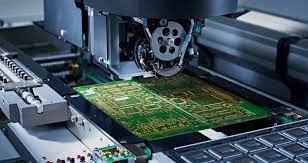
Once the PCBs are created, they are sent to an assembler for component mounting and soldering. This can be done using either surface-mount technology or through-hole mounting. In surface-mount technology, a thin layer of solder paste is placed on the assembled circuit board, and the component leads are then positioned on top of it. The assembler then uses a soldering tool to attach the components to the pad. In through-hole mounting, the assembler places the component leads into holes that were previously drilled on the bare circuit board. The holes are then plated with copper to create a conductive path.
How an Assembled Circuit Board Is Used in Mission-Critical Applications
Before the components can be mounted on the board, the layout must be checked for any mistakes. The assembler must also ensure that all the components are properly oriented, especially those with polarity, such as diodes and capacitors. It is important to mark these polarities so that the correct end is facing up. To make sure that the polarity of the components is consistent throughout the entire assembly, all pin 1s must be marked with a dot or number 1.
After the components are mounted on the board, it is passed through a reflow oven, where it is heated under controlled conditions. This heat causes the solder to melt and flow, bonding the components to the circuit board. This step is important to ensure that the solder can withstand the stress of high-voltage electrical gradients.
In addition, it is important to choose the right material for the circuit board substrate. The material must have a low dielectric constant, which determines the speed at which electrical signals travel through it. The material must also have a good trackability and a high-level dielectric breakdown voltage, which is the maximum amount of electric current that can be safely carried through the circuit board.
If your company needs a circuit board for a mission-critical application, you should work with a contract manufacturer that has extensive experience with Class 3 electronics. A reputable company will not only be able to manufacture your boards quickly and efficiently, but they will also help you design the board with manufacturability in mind.